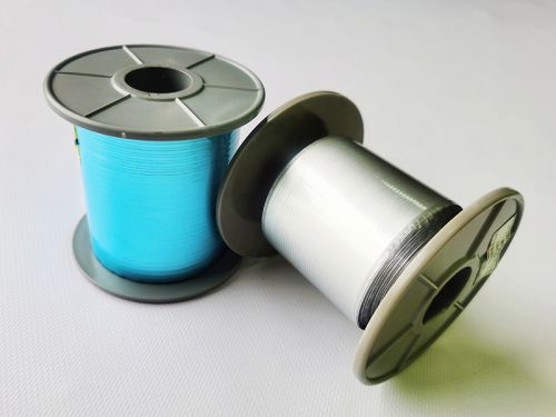
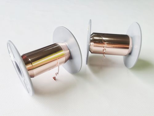
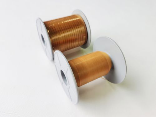
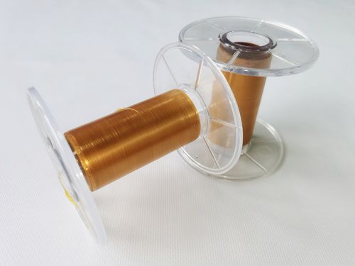
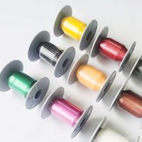
- Total thickness: (10μm to over 100μm) with a tolerance of ±3μm
- PI layer thickness: (≥2μm) + copper layer (≥0.1μm)
- Tensile strength: ≥30Mpa
- Width: 0.5mm to 990mm
- Elongation rate: ≥30% minimum
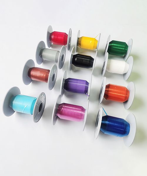
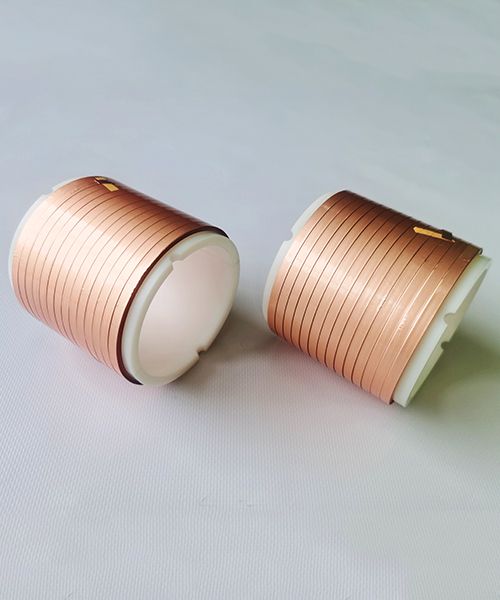
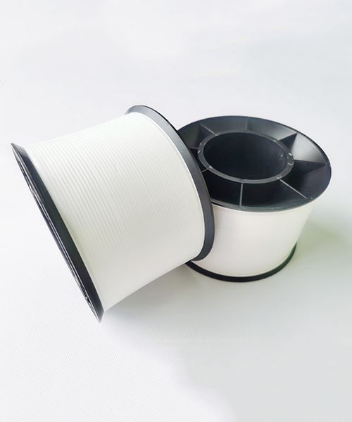
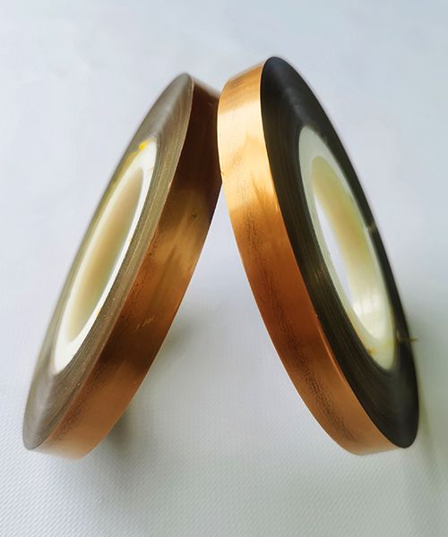
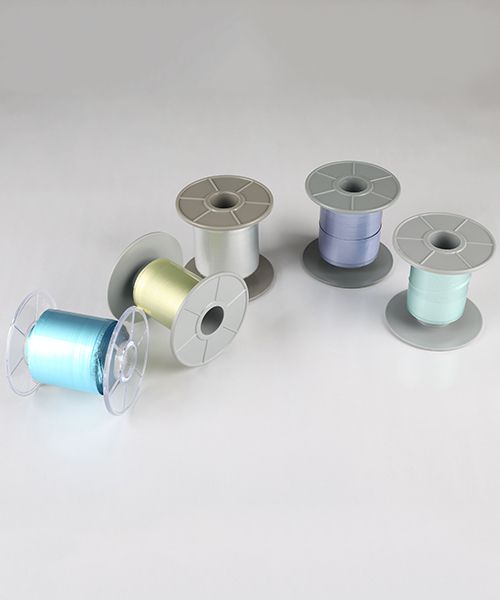
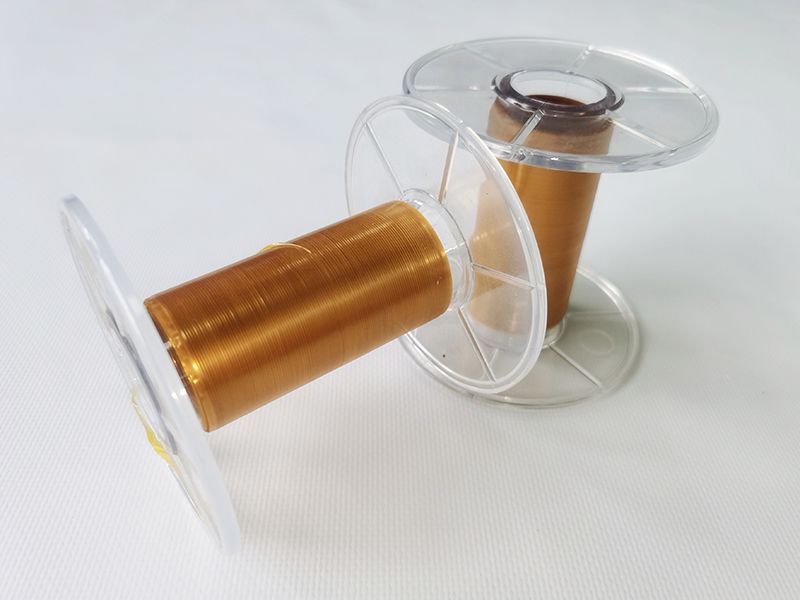
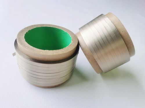
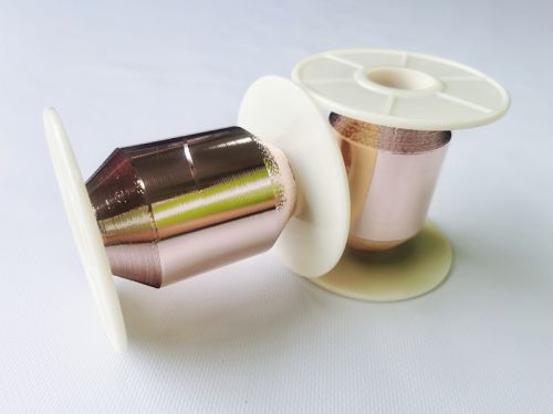
- Packaging: rolls (D30), sheets, 76mm removable rolls, inverted cone packaging
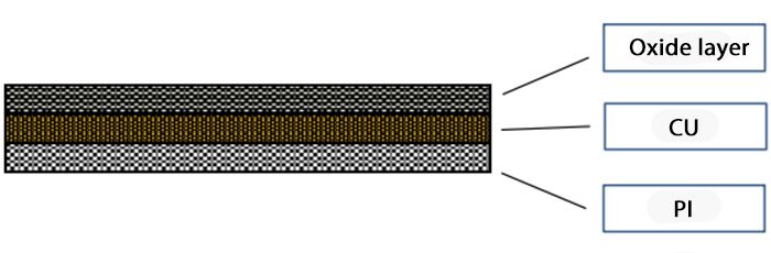
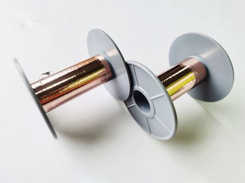
Copper metallized PI film is a thin film created using vacuum metalized on a polyimide substrate, known for its excellent adhesion and electrical insulation properties. PI plastic is among the most heat-resistant engineering plastics, with some variants enduring long-term exposure to 290°C and short-term exposure to 490°C. It also offers strong mechanical performance, fatigue resistance, flame retardant, dimensional stability, good electrical properties, low molding shrinkage, resistance to oil, common acids, and organic solvents. However, copper metallized PI film is not resistant to alkalis but boasts excellent friction and wear resistance.
- Ease of Coating
- Flame retardant, radiation resistance, and thermal insulation.
- High-temperature insulation
- High adhesion strength and dielectric strength
- Outstanding voltage resistance and tensile strength
- Perfect balance of electrical, chemical, and physical properties
- Thin and heat-resistant parts for fastening and electrical insulation
- Used in TAB bonding (tape automatic bonding), heat-resistant films, etc
- Flame retardant materials
- Thermal insulation materials
- Data transmission cable
- EMI shielding
EMI solutions include three main approaches: electromagnetic interference shielding, printed circuit board grounding, and electromagnetic interference absorption.
- Electromagnetic Interference Shielding involves blocking electromagnetic noise and attenuating cable-collected noise. It uses high-reflectance materials (usually low-resistance metals) to encase or seal openings in target devices for EMI and EMS solutions.
- Printed Circuit Board (PCB) Grounding refers to grounding electronic equipment electrically to prevent electric shock, treating the Earth as a massive conductor at zero electric potential. Two grounding methods are employed: frame grounding and signal grounding on PCBs.
- Electromagnetic Interference Absorption (EMI Absorption) utilizes magnetic loss, dielectric loss, and conduction loss to convert radio wave energy into thermal energy. EMI absorbers have a wide range of applications.
 Polyester Film Tape (PET Tape)
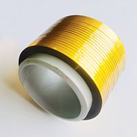 Shielding Laminates
 Vacuum Metallized Films & Fabrics